Sunday 28 December 2014

USB-UART control port

As part of my GSoC assignment, I tried to expose the control port via uart, in addition to control port via usb which was already present. I could not get it to work that time. So now I took the job again. Instead on working on my previous code, I decided to start with a clean slate.
My approach was to mux the already available resource which was being used for usb control port. After many hours of understanding the simulation waveforms, I finally managed to get things working, umm partially.
There are two kinds of commands. One which cause some changes for example forcing output video to be in grayscale, changing to HDMI0 etc. These are currently working in my uart control port. Then there are commands which output status back to the terminal. Now these currently don't work and I can get them working. The only problem will be that then the tools/fpga_debug will have to be written again for uart which will be plenty of work to do before sprints starts.

Wednesday 10 September 2014

Need for a remote access to FPGA

My mid sems finally got over yesterday and I got some free time in my life. So I am blogging. After completion of GSoC, lot of my juniors are asking me about my  project and a few seem to be interested. Few days back I answered a question on quora : http://www.quora.com/What-are-some-suggested-open-source-projects-in-Verilog-for-intermediates/answer/Ajit-Mathew and the person asking the question PMed me regarding my project. But what is stopping them from contributing is that they don't have an access to FPGA. In India, an Atlys board costs around INR 20K which is a big deal for a student. Also colleges have the old spartan 3 boards or don't give easy access to FPGA board.
I was recently talking to an alumni who is working in a FPGA based startup and he mentioned to me how they have created a hack which allows the developers to remotely access the FPGA, dump the .bit and see results. If we at TimVideos can develop a similar solution then it would improve participation greatly. If the logistics are handled, making this possible is not very challenging. Another solution can be to make a comprehensive test bench which allows black box and white box testing. A good language to create this test bench will be System Verilog as it combine verilog and class structure of C++. But this is a very big project. Creating accurate models for verification will take a lot of time.

The need to have expensive hardware for development is big disadvantage for open source hardware development. 

Monday 25 August 2014

Thank You TimVideos!

It is slightly late but better late than never. My final evaluation results are out and I have been given a pass grade by my organisation. It felt really good to see the mail of successful completion of GSoC after three months of hard work.
I would be very ungrateful if I don't thank my mentor, Joel "Shenki" Stanley. He is probably the coolest mentor and I have dibs on him if I participate next year. Initially I was worried as I didn't have a clear understanding of what to do and in those times shenki was really cool and motivated me which was a big help. I would also like to than our org admin Tim "mithro" Ansell, whose dedication to this org inspires me. Seriously, I would love to sit and talk with him on how he manages to motivate himself to learn and do so many stuff (BTW he works at Google).
I would like to keep contributing for the organisation as and when I get some free time. I also see a lot of my junior getting inspired and wanting to work for this org (one of them had sent a mail on the mailing list some time ago). I am planning to start a OSDG-Hardware group and introduce them to TimVideos. I see a lot of student interested to contribute but don't have sufficient knowledge about things relates to FPGA. So I will be soon (read "when I am free") posting some material and links which will help a raw student who knows only a HDL to become a "hardware developer". Another problem which I found when I discussed with my junior about open source hardware development is the need to have "the hardware" which for us in out case is the FPGA (very expensive considering a country like India). We can slightly mitigate this problem by developing a test suite which helps students who don't have hardware.
The journey of GSoC was great. I have was voted as the most hardworking GSoC intern among my friends who were also interning at GSoC orgs. My learning was really awesome. I feel smarter than most of my batch mates (which will slowly fade away when mid semester exams start). Also the exposure to open source community has restored my faith in humanity because good people still exist and that too in great number. Overall, this experience will remain green in my mind forever.

Monday 18 August 2014

GSOC Final Report

Result Summary

Timvideos is trying to develop an opensource video conferencing solution. The organisation has both a hardware component (HDMI2USB) and software component (like Gstreamer, flumotion). I was working on the hardware side of the org specifically on HDMI2USB fpga firmware. HDMI2SUSB is basically a solution based on FPGA to compress HD video stream input from a source like video camera and output the compressed stream via USB, hence the name HDMI2USB.

GOALS

My  project was on "Optimisation of MPEG Core". In the original firmware, the output stream from USB was about 10-11 fps which is very low and not suitable for video recording, the primary purpose of HDMI2USB. The aim of my project was to improve this frame rate. I had proposed to improve it to 60 fps @ 720p. As the reason for a slow frame rate was not fully understood, I built a lot of firmware to get the "status" of the HDMI2USB which later on became my second project, to create a "Debug Infrastructure" for HDMI2USB.

Final Outcome

Finally I was able to improve the frame rate to 30 fps (which is the minimum required for recording) and set a system which allows developers to easily output debug data via CDC or UART Port.

How did the frame rate improve?

The title of my project "Optimisation of MPEG Core" isn't a very apt title. The work I did tried to optimize the whole firmware. The original firmware has an image buffer which stores a frame before being compress by the JPEG core. The state machine of the image buffer was such that no processing was done when a frame was being read and no frames were read when processing was done. This was the bottleneck which was causing a slow frame rate. To remove this bottleneck I pipelined the read and write cycles of the image buffer. This reduced the number of frames which were being dropped and hence improve the frame rate.

Debug Interface

The debug interface is a new feature added to the HDMI2USB firmware. Unlike programming language which can be easily debugged using printf statement, systems on hardware like FPGA require elaborate methods. The debug interface which has been implemented allows data to be output via CDC port which was part of the original firmware and UART port which has been added to allow more options to developers and users incase CDC fails. Also a program has been included which reads bytes from fpga and presents them to users in a human readable format.

Heart Beat Feature

Sometimes when the image is static, it is difficult to tell whether the fpga firmware is working or it has hung. To remove this ambiguity, a heart beat feature was added which is basically a small block of pixel in the bottom right corner of the frame pulsing at a constant rate. This feature can be turned on/off using a hardware switch and via the CDC control port.

Community Outcomes

The Timvideos developers’ community has promising outcomes after completion of this project. The biggest being the HDMI2USB can be used for recording. Now that HDMI2USB firmware streams at 30 fps, it can be used for recording at 30 fps which is the minimum frame rate required for video recording. Also, I may not have been able to meet the 60 fps as I mentioned in my proposal but I have successfully revealed some issues in the HDMI2USB firmware which need to be dealt with, most importantly the bandwidth of FX2 chip.
There are certain other features which can be implemented but have not been implemented due to lack of time like reducing subsampling to 4:2:0 and implementing a triple buffer in the image buffer. This may or may not change the frame rate but it will be interesting to see the outcomes if they are implemented. The debug infrastructure that has been setup will allow future developers to easily debug the hardware and also provide an easy way of troubleshooting for future users. Addition of UART allows multiple debug/control option incase cypress fx2 fails.  As my project dealt more with optimisation which involves getting a good understanding of the system as a whole, I have gained good knowledge about the fpga firmware. This will be useful for future developers as I am in a position to be able to guide them regarding specific issues. Also thanks to the exposure I received due to this project, I have started a Open Source Hardware Developers Group in my university where soon I will be introducing TimVideos. Hopefully this will increase the number of developers for HDMI2USB.

Replicating Results

All the code relevant to the project has been merged into the HDMI2USB repository.
Also check out the how to use section in the following blog posts:

Bugs/To Do

  • Support 1080p via USB: I successfully added 1080p test pattern (Hidef snow) to the hdmi2usb. It was streaming out of the HDMI port but not out of USB. Here is the video.
  • Add Control Port via UART: I was able to expose some features of control port to UART but not all. I will try to finish after GSOC.
  • Automatic Encoding Quality Control: It has been noticed that the encoding quality depends highly on the type of image. So there can be a auto encoding qulaity control like the one in youtube (it changes the resolution though) which allows more compression if the frame rate is slow.

Documentation

Developers Guide has been updated to reflect new changes.

Learnings

This project has been a great learning curve for me. My knowledge about fpga and related stuff has increased exponentially. The mentors are great and supportive. Working for this org was a great introduction to Open Source Development. I would highly recommend the org to anyone who is new and wants to get dirty with FOSS.

Heart Beat Feature

If a static is being displayed by HDMI2USB (for example a slide in a presentation), then it is difficult to tell whether the HDMI2USB is working or it is hung. So a heart beat feature has been added which causes a block of pixel to pulse in the lower right corner of the screen indicating that HDMI2USB is alive.

How to control?

Heart Beat (HB) can be switched on/off using switch SW 0 or using the CDC control port by sending ASCII command "S(s)" and "H(h)". But the control port will work only when the switch is on. So the switch acts as a "hard off" signal.

How to tweak the pulse?

The heart beat module is instantiated in the image_selector module. To change height, width and pulsing rate of the pixels, change the generics HB_length, HB_width and alt_aft_frame in hdl/misc/image_selector.vhd file.

Video

Sunday 17 August 2014

Debug Infrastructure Documentation

Debug infrastructure provides an easy interface for a developer to output data from the FPGA board for debugging. It is also useful for end users in case of troubleshooting.

The BIG PICTURE:


The debug data is collected into the debug_module which then breaks the data into bytes and sends them to UART module and USB_top module. These module send data via CDC/UART to host.

How to use?

The output of UART/CDC are bytes. So to convert them to human readable format and hence allow easy debugging, a program fpga_debug.c has been provided which reads data from the fpga and then outputs data in correct format.

To compile fpga_debug.c
> cd tools
> make

To run debugging program
> ./fpga_debug

How to add new debug data? 

  • Route the data into debug_module
  • Break it into bytes and add to uart_byte_array
  •  Change value of "constant N_BYTES  : integer" appropriately
  • In fpga_debug.c add code to parse and output the new data
You are done!

Output Bytes:


Byte
Description
1
Device State
5:2
Resolution of Source
6
Input frame rate in fps
7
Output frame rate in fps
8
Frame write time in ms
9
Frame Processing Time in ms
10
No. of frames dropped for every frame processed
13:11
No. of bytes in a frame


NOTE: To use UART port, exar device driver should be installed. But the driver does not allow CDC port to function along with it. So you can use either UART or CDC but not both.

Video


Monday 11 August 2014

Thursday 7 August 2014

Control port via UART

This is turning out to be more difficult than I thought. I was trying to use the same controller module for cdc and UART. But for some reason which I haven't been able to figure out, the video output is null when I am trying to do that. Tried a bunch of stuff but nothing worked. I guess I will have to make a separate controller for UART.

Tuesday 5 August 2014

Hidef snow working!

Finally got the hidef snow working through hdmi2usb via HDMI out but not via usb.
I am getting a timeout error. I increased the watchdog timer inside the usb module to absurdly large value but it still did not remove the error. The large size of frame might be the problem.

Friday 1 August 2014

Unable to get hidefsnow working

I wanted to add a 1080p test pattern to firmware so the performance at  that resolution can be understood. Unfortunately things are not working. I am getting strange output values from debugger. Hopefully I get it done soon.

Wednesday 30 July 2014

Lot of pushing done

- Debug Infrastructure Pushed
- Pipelined Memory Pushed
- Will do heart beat tomorrow

Friday 25 July 2014

Daily Snippey

Debugger program with cdc in done
H2u firmware with cdc debug done with timing errors. But it works. Worked really hard on it but did not meet timing.
Memory pipelining done for all encoding quality.
Today (Saturday) we have a Church outing so I will fix everything and commit them on Sunday.
Cheers!

EDIT: The title was a typo because I was using my tab. But it sounds cool.

Tuesday 22 July 2014

Daily snippet

Oops missed yesterday's blog.
- Heart beat feature completed
- Sent debug data out of cdc
- working on debugger program
- major changes to debug module

Friday 18 July 2014

HDMI2USB Serial Controller Port

When we connect HDMI2USB to host, two CDC are enumerated. One is for UVC(ACM0) and the other is for controller port(ACM1).
The controller port can be used to control certain features of HDMI2USB and also display status of USB, jpeg encoder etc.
To access this use any serial terminal program like gtkterm. The commands send to the control port is in ASCII. The ascii commands are two byte, first is the address(like U or u for USB TOP) and the second is the command you want to send to that address (like S or s for status). So if you send US, it will return the status of the USB Top module. Since the terminal I am using allows only hexadecimal commands, so I have to convert the ASCII commands to their hex equivalent (which is irritating).

While creating the debug infrastructure, I completely neglected that there is already a lot of infrastructure already built in due to the control port. Some feature that I have added like frame rate etc can be exposed via the control port. Then we can have a debugger using the control port. Plus it can be used to control features of firmware which is even more awesome. What say mithro/shenki?

Controller Port

I fixed up Heart Beat module as Karl required it. Mithro asked me to add functionality to turn it off/on using controller port. To do that I dug through the code of how data is send through the second ACM port that is enumerated via HDMI2USB. I was finally able to do it.

Thursday 17 July 2014

Daily Snippet

Instead of two encoder, I tried changing the state machine to drop frames as low as possible but it didn't work. Will try to work on it tomorrow.
Also I changed the code of the heart beat feature I had implemented long ago. I did not have atlys board when I implemented it so came to know about a bug in the code when I ran it on the board. Eventually was able to fix it and improved the code to use lesser number of flops.
Also mithro added me to the TimVideos Hardware hacker team. It felt nice, actually very nice. It actually felt like this:

So can I now update my linkedin profile? But before that let me learn Git coz when shenki talks about stuff like bisecting, rebase I am like this


Wednesday 16 July 2014

Debug Program almost done!

The bare bone debug program is ready.
Here is how the program looks like. Things will improve as other developers add stuff to the debug infrastructure like packet count, expansion boards ID etc.
There are two bugs which I couldn't fix even after hours of attempt: 
  • UART is suddenly send incorrect data causing wrong output for a moment.
  • HDMI 1 is shown connected even though only one is connected.
I will spend some more time on it in the weekend.

Tomorrow I am planning to go back to the real stuff I am working on. Tomorrow I will try to add another encoder. Let's see if it is possible. If not, atleast we will know that this solution is not possible for available fpga resource.

Till then I am going to sleep.

Tuesday 15 July 2014

Oops Forgot again

I usually write my blog before going to bed. Yesterday I went to bed and then I realised I forgot to write my snippet. Now I had a very tough choice to make-"Sleep,blopost,sleep,blogpost" Finally I chose sleep. So now I wake up and write my blog.
Daily Snippet:
1) Removed some bugs from the debugger. (Behold the irony)
2) Added non blocking keyboard IO.

Hopefully I complete it today.

Phew, now I can sleep in peace.

Monday 14 July 2014

GSOC ain't your College Assignment

Today I submitted my first c code and it was a such a disaster that I am looking back and laughing at it. Contributing to open source comes with it's own baggage like license, coding style and git, all of which I never cared about. But these are very important in an collaborative environment and hence important to learn. I got the bare bone version of my debug program working (with errors) and committed it. But before committing I remembered, "Where is the license?" So I copied the license from a VHDL file ( I know I am a smartass) and then happily committed it, feeling proud of my achievement. Only later I realised that it won't compile because to comment in VHDL we use "--" which will throw a compile error in C. Shenki must have been ROFLing on seeing it.

Also I would like to propose daily tweeting instead of daily blogging. I haven't been blogging lately not because I was not working but blog, don't know why, sounds to  me hard work, like the daily cursive writing my Mom used to make me write when I was a kid.

Okay now I am rambling. Daily Snippet:
-[code]Debug program
-Studied Git
-Studied Linux Coding Stlye Guide
-Sat and wondered why mithro and shenki work so hard?

Tomorrow:
-[code]Debug program
-work on comments and *try* to rebase 


Sunday 6 July 2014

Plans

I would like to make hdmi2usb usable for 720p atleast.  Since we have already achieved 30 fps, things are looking good. Now the next thing to work on is finding an optimum encoding quality so that the encoded frame fit the fx2 bandwidth and are viewable.

Tariq observed that we are clocking pixels which do not have useful data. I would like to check that too. It most probably will not affect the frame rate but it might effect things at higher resolution.

How did fps improve to 30 fps?
In the original read/write state machine of DDR, read and writes did not happen simultaneously. I modified the read and write state machine to start encoding as soon as 8 lines are read into the DDR. This allows encoding of every alternate frame and hence fps of 30. In case Shenki you want to test it on your system, then here is the xsvf file.

How things can be improved further?
  • Double/triple buffering: Can improve the frame rate to the maximum frame rate of the encoder(currently it is 40 fps).
  • Using two encoder instead of one: Now as every alternate frame is being dropped, another encoder can be used to process these frames. This way we can get fully 60Hz frame rate. But there are issuses:
    •  Already the encoder is taking up almost half of the BRAMs available. So there might not be enough space for adding another encoder or if it is possible to add another encoder, there might not be enough space for other features which are going to be added.
    • As two encoded frames will be produced simultaneously, an way to send these to host via fx2 has to be designed which in turn will cost more memory.
  • (Suggested by shenki)Removing DDR image buffer and storing frames directly into the line buffer: I am not sure if it is possible. Wil have to check.
  • Subsampling: Currently the encoder takes in RGB888 and converts into YCrCb and then subsamples it at 4:2:2. This can be changed into 4:2:0. This can reduce encoding time and might help us with the bandwidth issues. 

Wednesday 2 July 2014

Daily Snippet


  • Completed mid term report
  • Studied about DDR2
  • Studied about double and triple buffering. Here is an excellent link to the same. http://www.anandtech.com/show/2794/2
  • Tomorrow I will try to change the image buffer SM such that encoding starts as soon as 8 lines are written into DDR. If this works frame rate should increase.

Tuesday 1 July 2014

Daily Snippet

  • Finally got the frame size of compressed image from the UART port.
The results confirm that the slower frame rate for higher encoding quality is because of bandwidth issue.

For 50% encoding quality, size of encoded frame is .436MB. So if the maximum bandwidth of fx2 is 40MBps then maximum number of frames possible is 91 which more than what we require.

In case of 100% encoding quality, the frame size of encoded frame is 3.6 MB which is greater than the input frame size. This is possible because in RLE, if there is no repetition of data, the size of encoded image can be double(wiki page). So for this size and a bandwidth of 40MBps maximum frame rate is 11 which is also observed.

So there is also a need to find an optimum encoding quality which has reasonable image quality and size.

  • Started working on mid term report. Hopefully I will finish tomorrow.
  • I am facing an issue with mu laptop. It turns off because of excessive heating when I build the firmware. This was not the case earlier. This wasted a lot of my time yesterday and today. I am using ubuntu 13.10. If anybody has any idea about the problem please help. Right now I go to windows build the firmware and then use ubuntu for rest of my stuff.

Friday 27 June 2014

Debug Data

Things are not as easy as they seem to look. After plenty of debugging and testing on hardware I was finally able to get the debug code working. I haven't implemented the part which outputs size of encoded data because it is a 3 byte value and I didn't have the foresight to write a very generalised code. Other debug data are 1 byte.

So this is what I get from the UART. By the way I am using the test image and encoding quality of 50%.

  • Input Frame Rate: 60 Hz. This is what it is suppose to be.
  • Output Frame Rate: ranges from 15 to 21. So lets take the average value to be 18.
  • Time taken to write frame into DDR2 Ram: 16-17 ms. This is what I approximated
  • Time taken for encoder to compress: 23 ms Again I was close
  • No. of frames dropped: 2
So in a second is 60 frames. And for every frame read, 2 frames are dropped which means only 20 frames are being processed.

Writing + processing time = 40 ms => 25 fps. So I *guess* we are losing 10 milliseconds in sending the data. (will check this).

So I guess we know what our bottleneck is : When image is written into ddr2, it is not processed and when image is processed, image is not written into ddr2.


Wednesday 25 June 2014

Daily Snippet

  • Got the UART working: The uart of atlys without the vizzini driver enumerates as ttyACMx. Rohit was able to use it to send data but I was getting crap values. Turns out that you can only send data from fpga via this and not send data to fpga. My uart test code would echo back the byte sent and since fpga did not receive anything I got crap values. This wasted a good 2 hours of my life.
  • Shenki's UART driver is working: To install vizzini I have to first remove cdc-acm which I did not do and hence  it did not work initially. Then after reading carefully the README I was able to get it working. The uart enumerates as  ttyUSB0. 
  • Tested my code: My code was working in part, did some correction. But yesterday  there was power cut even in the evening so couldn't do much work. So I will be travelling to my parent's place today and work from there till things become normal here.
Sorry I missed the deadline. Will complete it ASAP.

Tuesday 24 June 2014

Daily Snippet

  • Coded debug firware, almost done. Pushed to my gsoc branch.
  • Design Documentation
  • Testing UART, worked for Rohit not working for me(grrr)

Sunday 22 June 2014

I think I have some idea on why frame rate is slow. In my previous blog I explained how the state machine of image buffer works. Basically, a frame is stored first and then read into encoder for compression. From simulation data, a 1024*768 frame takes approx 25 ms (@ 78Mhz) to compress a frame. But if the frame rate of the HDMI source is 60hz then the minimum time taken to write a frame into the DDR2 Ram is 1/60s ie 17ms (assuming it takes no time to transfer data into DDR2 RAM which ofcourse is not true). So it takes 42 ms to store and compress a frame which gives you a frame rate of 23 fps. There is no pipelining between frames.

In simulation, the encoder is fed with new data if its buffer is not full. But in actual firmware, data needs to be accessed from DDR2 RAM which even though is small is not negligible. Also the raw image data is buffered before being written into RAM to prevent loss of data, so it takes far more than 17 ms to write the whole frame into RAM. So my guess is frame rate of DDR2 + encoder system is around 20 fps.

Also, I ran test bench for different encoding qualities. Turns out that for 100% encoding quality, the compression ratio is around 5-6 whereas for 50% encoding quality, the compression ratio is as high as 20-25.

So output size of a frame at high encoding quality:
1024*768*24/5/1024/1024=3.6 MB
Now bandwidth of cypress fx2 is 40 MBps. So  fps in high quality case will be 40/3.6=11.11 fps. That's why changing the frequency did not change the frame rate(I guess).

In low quality case as the compression is high, fx2 bandwidth does not limit the frame rate but the firmware limits the frame rate. So the observed fps is around 18.5-19 which is close to the fps I am guessing using calculation.

Friends, Romans, Mentors and countrymen please comment.

Disclaimer: I have used a lot of handwaiving calculation. So if I have used too much liberty please comment on it. I will try and give rigorous  maths.

Friday 20 June 2014

 Today I planned to complete the simulation of HDMI2USB but it turns out that the calibration_done signal is not yet high( it has been 6 hours now). I tried changing the tb, using some advance options like Joelw suggested but nothing seems to work. So I am either doing something terribly wrong or it is supposed to take a lot of time. So finally I decided to use pen and paper and try understand the code. It took me a lot of time because VHDL by nature is concurrent  and I had not fully understood the working of Xilinx MCB but I guess I have done it correctly. Turns out that image buffer works fine.

The DDR2 read and write state machines are pretty complex because in general memory controller are complex. From what I could comprehend, there are three state machine in image buffer of HDMI2USB, one read from the RAM, second writes into the RAM and the third which controls the read and write state machine.

The third state machine looks something like this:
1) Wait for start of frame
2) If start of frame is detected, start writing the frame onto RAM until end of frame is detected (wr_img=1)
3) Once end of frame is detected, send start command to JPEG encoder and wait for "Jpeg is busy" signal(wr_img=0)
4) If "Jpeg is busy" detected, start reading from RAM till the entire frame has been read(rd_img=1)
5) Wait for done signal from encoder.(rd_img=0)
6) Go back to step (1)

I don't think read and write can be pipelined as DDR2 Ram do not allow simultaneous read and write.

Here the only optimisation I can see is that instead of waiting for done after completing reading of frame (step 4), the state machine can wait for start of next frame and start reading.

To understand the read and the write state machine, I dug the data sheet of MIG.
Read state machine looks something like this:

1) RESET: Wait for calibration to be done.
2) read_cmd: if rd_img=1. Put read command and address into the command fifo.
3) Wait for read data fifo of RAM to fill up. (64 words)
4) Once full, send the data into JPEG buffer if the Jpeg buffer is not full.
5) If 64 words are read goto step (2)

Write state machine:
1) Wait for calibration
2) If wr_img=1 and there is something to be written fill the write data fifo of RAM(64 words)
3) Once full, push write command and address to command fifo
4) Wait for write to complete.
5) Once done goto 2

The raw rgb data from image selector is first buffered using fifos and then sent to RAM. This helps prevent loss of data but adds to the latency.

Everything seems to be legit. Only optimisation I can see is that instead of one read port, two can be used to pipline read cycles. So when one read data fifo is completely read and there is still space in the JPEG buffer, data from second read data fifo can be used. But since this is a DDR2 ram operating at 325 Mhz read time from RAM to fifo should not be great, so using two ports won't change much.

Also, an inherent problem with the jpeg algorithm design is that 8 lines are required to start encoding. Since processing of frame is not pipelined as seen above and after processing of a frame the system resets, for a resolution of 1024x768, in every frame there is a stall of 1024*8 cycles.

Tomorrow (I mean today) I will try to test the bandwidth of USB. This article says maximum throughput is 40 MBps. So for 30 fps frame rate of 1024x768 resolution frames, the minimum bandwidth (assuming compression ratio of 10) should be (1024*768*24*30/10)/1024/1024 = 54MBps. Am I missing something?


Thursday 19 June 2014

Today I completed the coding part for the simulation of HDMI2USB. The main aim for this was to check whether the read and write pattern used in DDR2 Ram is optimum. For this I removed all the parts which did not affect the read and write performance of DDR2 Ram like EDID, USB etc. The  only problem is that the simulation takes up a lot of time. It takes upto 4 hrs for the calibration of DDR2 ram. I am currently simulating it. I will wake up and check the waveforms.

Wednesday 18 June 2014

I'm Back!

Finally I am back from my trip to US. The competition didn't go the way I wanted it to be. Our cansat did not send any telemetry. Also it landed in a sunflower field which meant we could not recover the cansat and the onboard memory which had all the telemetry data. But it was a good learning experience, plus I got a chance to meet people from all over the world which was great.
I will resume working on the project. I will continue my work on simulating the HDMI2USB firmware. Hopefully, I will be able to come up with something fruitful by the end of this week.

Friday 6 June 2014

Used Joelw's code on his blog to test the DDR2 ram. After initial hiccups I was finally able to do it. Also I underclocked the DDR2 Ram to check if there is a change in frame rate. When clock was reduced by half there was no change and when I reduced it further mplayer showed a timeout error.
@shenki: I have added a new commit with the xsvf files. Try them on your board and please tell me the frame rate you observed.

Thursday 5 June 2014

Daily Snippet

-Studied ug416 and ug388 to understand XILINX MIG
-Studied working of DDR2 Ram
-Ran example design to understand the working further. Took me lot of time to get the clocks working at correct rate as PLL values were changed manually which I didn't take notice of.

The read FSM of DDR2 looks something like this^. So 1 burst read gives 64 bytes. Jpeg encoder needs 1280*8*3 bytes to start. That means it takes a lot of cycle to fill the jpeg. I will try under clocking the DDR2 ram today and see whether it affects the frame rate.

Also I will start coding the test bench.

Wednesday 4 June 2014

Daily Snippet

As I am planning to write a test bench to simulate HDMI2USB, I spent most of the day trying to understand the TMSB protocol as I had not encountered it earlier. I was finally able to write a code which generates TMSB signal given RGB values.

Work for Today: Understand the working of DDR2 ram and simulate it successfully. Then I will be ready for simulation of the whole.

Tuesday 3 June 2014

UART Documentation

Atlys board has a UART-USB bridge which can be used for UART communication with other devices. UART is useful as a debug so I have made a simple UART.

Features:
1.Variable Data Bits: 7, 8, or 9 data bits and 1 or 2 stop bits
2.Parity generation and checking: odd, even, or none.
3.One transmit and one receive data buffer.
4.Received data and status can optionally be read from a single register
5.Built-in Baud Rate Generator.
6.Variable Baudrates. Use case: 19,200
7. Data is received in frame.

Architecture
UART Transmitter
 It has 3 major components:
1.FIFO Buffer
2.Baudrate Generator
3.Transmitter interface circuit

UART Receiver:
 It has 3 major components:
1.Baudrate Generator
2.Receiver interface circuit
3.FIFO Buffer 

Primary Inputs/Outputs
Inputs
1.clk,reset
2.WIRE[7:0] W_DATA - DATA INPUT TO TRANSMITTER FIFO
3.WIRE Wr_UART- WHEN SET TO HIGH W_DATA IS WRITTEN INTO TRANSMITTER FIFO 
4.WIRE Rx - UART RECIEVER LINE
5.WIRE RD_UART- READS  THE DATA FROMP FIFO
Outputs
1.WIRE TX_FULL- HIGH WHEN TX FIFO IS FULL
2.WIRE TX- UART TRANSMITTER LINE
3.WIRE RX_EMPTY- HIGH WHEN RX FIFO IS EMPTY
4.WIRE R_DATA- OUPUT FROM RX FIFO

FSM for Reciever


As the communication is asynchronous, data is oversampled. Each bit is oversampled 16 times. Oversampling is done using a mod m counter.
As the circuit is oversampling, I am running UART at 50 MHz which is generated using PLL.

How To Use?

  • Add UART files to your design file.
  • Add UART_clock.xco. You may have to regenerate the core depending on you design.
  • Set paramerters of UART_main.(The following are default parameters)
    • Data_Bits=8                  // No. of data bits
    • StopBit_ticks = 16        // No. of ticks for stop bits. 16/24/32 for 1/1.5/2 bits
    • DIVSIOR = 326           // Use it to set baud rate. Divisor= 50/(16*BaudRate)
    • DVSR_BIT=9              // No. of bits of Divisor
    • FIFO_Add_Bit= 2        // No. of address bits of FIFO
  • To transmit data, drive w_data and strobe the wr_uart signal.
    • Data will not be written into fifo if tx_full is high
  • To dequeue data from receiver fifo, strobe the rd_uart signal. 
    • Data in receiver is invalid if rx_empty is high
  • Add the following lines to your ucf file.
  • Download exar driver from here and install them. 
    • NOTE: Turns out that the linux drivers are outdated. Shenki has made changes to it which can be found here but I was unable to get it running. I have test the code on windows.
  • Use hyperterminal or gtkterm to monitor/send data.
  • Enjoy!
  •  
    You can get uart files from UART folder in this link:

Monday 2 June 2014

Daily Snippet

  • Wrote a code to test the UART on hardware
  • Wasted a lot of time trying to get the driver running. Shenki changed the source code to make it compatible with latest kernel but my terminal hangs when I install the drivers.
  • Finally tested the UART using Windows. Working!
  • Tested the code for different baud rates. Working for 19200.

Tomorrow:
  • Integrate the code with HDMI2USB and test it.
  • If things work, write documentation and give to HDMI2USB community to test.

Sunday 1 June 2014

Weekend Review

Work done in last week:
  • Investigated the effect of encoding quality.
  • Investigated the effect of post jpeg stages
  • Changed FSM of JPEG core
  • Underclocking of Jpeg core
  • Studied Chroma Subsampling
  • Wrote code of UART (alpha stage)
Work to be done this week:
  • Complete UART implementation with documentation on how to use it so that it can be used by other developers.(2-3 days)
  •  Then try one of these: 
    • Investigate performance of pre-jpeg blocks.
    • Write a test bench to simulate the HDMI2USB firmware.(Will take a week or two).
    • Implement chroma subsampling 4:2:0.

Friday 30 May 2014

Snippet

 Today
[Code] UART done with Testbench

Tomorrow:

Test it on hardware

Thursday 29 May 2014

FSM Changed, FPS Did NOT!

I changed the FSM which controls the JPEG encoder yesterday. I initially went in the wrong direction as I understood the OPB protocol incorrectly. When I finally understood the problem, the implementations was of few lines. Earlier quantisation tables were written every time a new frame was loaded. Now it will change only when encoding quality changes. So it saves 1024 clock cycles per frame if encoding quality does not change. It took me several attempts to get it working. But FPS didn't change. It will probably make a difference when the fps is very high, so the clock cycle saved per frame will be significant.

Also, I tried underclocking. I changed the clock divider of jpeg clock(freq=625Mhz/clock divider) from 7 to 11. FPS did not change for 7,8,9. But I got timeout error for 10 and 11 which I guess means FPS was too low. I honestly don't know what to make out of this.

Also there is a bug. I have no idea about the bug. Here is the video.
 bug video
In the video, things worked after two attempts but it can take more. .

Today I was supposed to start changes chroma subsampling of the encoder but I guess adding UART functionality would be better as it will help me and other developers to debug easily. So I will spend the day trying to get the UART working on the board.

Snippet:
Work done- Changed FSM, Played with underclocking, Studied chroma subsamling
Work to be done today-
- Implement UART on board


Wednesday 28 May 2014

Yesterday probably I worked the longest (10 hrs maybe). I was trying to check whether the reason for slow fps is blocks after jpeg core. To check this I removed the the signals which the usb controller gave to the jpeg core. Also I wrote a code which counts the done signal of the jpeg core and I output the range of the count using LEDs(like for count less than 10 LED0 would light up). And it turns out that count of the done signal was in same range as the output fps. I tried different combinations like different encoding quality, allowing some signals of usb controller to control the jpeg core while ignoring other and the result was more or less the same. Meanwhile the code threw a timing error which took me 2 hrs to debug. 

 Also I did some reading on quantisation tables for JPEG. Turns out that quantisation should be low for luminance table (quality-85%) and high for chrominance of around 50%. But this is a general rule and cannot be used for all applications.

Today I plan to change the jpeg top module and see whether it improves fps. I have few ideas.

Tuesday 27 May 2014

Finally the FPS changes!

In my previous post I mentioned how it appears that JPEG encoder is working at 100% encoding quality. Turns out it is true. I hardcoded to make the core run at 50% quality and 100% quality and there was a clear change in the fps. At 100%, the fps was same as the normal HDMI2USB frame rate. And at 50%, framerate jumps to around 20 fps.
Now 100% quality encoding is not good.Why? In the quantisation step, a each sample of a 8x8 block is divided by a number which depends on encoding quality and frequency component the sample. Human eye is sensitive to low frequency so in quantisation process, low frequencies are preserved and high frequencies are suppressed. But when for 100% quality all components are preserved, so the output file is large but for the human eye it looks as good as say 75% quality.
Plus at 100% quality, the clock cycles spent on quantisation are waste as we are basically dividing by 1.  

 (^100%-11.50 fps)
(^50%-19 fps)

I will look up some material on chrominance and luminance tables and see what is a good trade off between quality and frame rate.


Monday 26 May 2014

Today I tried to change the encoding quality manually. The reason for this is that if the jpeg core is running at 100% quality then the quantisation step of JPEG encoding is useless. For that I changed the code of JPEG top and used switched in board to select the encoding quality. Unfortunately after flashing the firmware, mplayer and guvcviewer could not play the HDMI input. Things are going slow because it takes around 15 mins in my system to generate the bitstream. I will try to get things working tomorrow too. If things don't work, I will reach out for help.

1 Week Down!

In the past week I stuck to my goal of improving the fmax of MPEG coder. I tried to run at 105 Mhz(because clock dividers should be integer) but timing constraints failed. Tried a bunch of stuff but didn't succeed. Then I finally ran the MPEG  core at 90 MHz. All timing constraints were met but there was no improvement in the speed which was a bummer. Anyway during weekend I tried an optimisation but was not able to run it successfully on the hardware. The JPEG top module has the following FSM


As you can see, after every frame compressed lumination and chrome tables are written again. Plus because of the OPB interface, there is atleast a cycle long wait for ack. So for every frame 512*2=1024 cycles are wasted when a frames is compressed. So I was trying to change the FSM so that the table writing step is bypassed if there is no command to change the encoding quality. Unfortunately my changes are not working on hardware. I am planning to spend some time on it. Also I plan to check the efficieny of HDMI2USB minus the cypress firmware so that I can test whether or not the cypress is slowing down HDMI2USB. Finally I am planning to start modifying the code for 4:2:0 sub sampling. This will take some time as I need to rewrite the FSM of JPEG core. This will probably take 2 weeks. Hope this week gives me some positive results.

Friday 23 May 2014

As it turns out, the JPEG encoder works at 78 MHz. As I didn't have a oscilloscope, I wrote a VHDL code too check the frequency of the PLL using LED. And yes, it turned out to be greater that 70 Mhz. So my theory that the core is running slow because the clock is slow turns out to be false. I did run smartexplorer to remove see if I can remove the timing faliure but it didn't. Further analysis revealed that I can safely ignore the path that was failing timing constraint as it was the PLL MUX selecting signal which was not important. I used a TIG in the UCF file to remove it. I changed PLL parameters to make the encoder run at 100 MHz, and strangely ISE did not throw any timing violation but things didn't work on hardware. I will try once again in the weekend. I use guvcviewer to check the frame rate of the video streaming and it comes out to be 12 fps on average. I will study other parts of HDMI2USB and try to find the bottleneck. 

Wednesday 21 May 2014

Clocking of HDMI2USB

Today I spent almost my whole day trying to understand the clocking of the HDMI2USB. Well it turned out to be a tedious deal because the firmware is in VHDL spanning arcoss multiple files and it has a memory interface which is generated using the MIG tool. THe MIG tool is very poorly documented. Thanks to a blog post by Joelw (http://www.joelw.id.au/FPGA/XilinxMIGTutorial) things got slightly easier. So basically, the oscillator output (100Mhz) is connected to the memory interface which has a PLL and this PLL generates 6 clocks. The first 2 clocks are used by MSB and the rest are for user fabric. The PLL parameter used in HDMI2SB is same as given in the blog. So except the image buffer which is the DDR2RAM, rest of the blocks of HDMI2usb run on 78.125 Mhz clock.
But something that caught my attention was this line from the blog

wire c3_clk0; // 32 MHz clock generated by PLL. Actually, this should be 78 MHz! Investigate this.

c3_clk0 is the clock driving rest of the HDMI2USB blocks. If it really working at 32 MHz then we actually know our problem.

HDMI2USB is currently working at 15fps for 720p. The JPEG encoder in simulation works at 20fps for a clock of 100MHz and the image resolution being 1080p. So it should work at ~50fps for 720p images @100Mhz. So if the JPEG encoder is made to run at 32Mhz clock, frame rate will be 16fps.
So if the PLL output is actually 32Mhz as written by Joelw then we know what our problem is. If PLL output is 78 MHz then I can't say what the problem is. It might be that the problem is not with JPEG core but something else. Anyways I have pinged Joelw about this and waiting for his opinion. Tomorrow I will try investigating this. Let's see how it turns up.

Tuesday 20 May 2014

Board Working!

Finally got the board working. I had initially used Adept and fxloader to flash the firmware but it turns out there seems to be a problem with fxloader. So I used libFPGAlink. I used the wiki by mithro on the same and after some efforts things starts to work.

(Lets ignore the tooth brush)
Now I am planning to try to improve the frequency of the operation of the JPEG encoder. Simulations show that at 100Mhz, 20Hz can be achieved for 1080p images. I am planning to run smartXplorer on the design and see which mapping and PAR strategy is the best. Also I will try to removing the timing violation as ISE slows other parts of the design to meet the timing requirements. So lets see how things work out.

Saturday 17 May 2014

Failed to get the board running!

I came back to college. A friend of mine was kind enough to lend me his HD monitor for the summer as he will be interning in Japan. I usually work do my fpga stuff on Windows but as everyone in the org uses linux I installed ISE on ubuntu. I did receive my board last week and was planning to get it running by the end of this week. Unfortunately I couldn't. I was able to successfully complete the flashing the FPGA with HDMI2USB firmware using Adept tool and generate test pattern on the monitor. Then I flashed the Cypress Fx2 chip with HDMI2USB firmware using the latest version of fxload. But when I tried the dmesg command, the output did not show HDMI2SB as aUSB device.
Posted the problem on irc, waiting for some help.

Test image 

Tuesday 13 May 2014

Work done part-2

New day!  New blog post!

This post will describe the last idea in my head which I did mention in my proposal but has a serious con. But this idea suddenly seems to be an attractive option as the limited BRAM memory seems to be a problem.

The idea is basically to divide the picture into two parts and then process them simultaneously. Send them two computer and then stitch them together.

(Taken from my proposal)

This has two advantage:
1) Currently 1 buffer of 16 lines is being used. To implement this I need to split the buffer into half. So extra input buffer is not required but an extra output buffer will be required in case the right half of the image gets processed first.This buffer will obviously be of smaller size as it is storing a compressed image. Of course, some extra pipe lining buffers will be added due to an extra  jpeg core but the main reason for increased memory utilization the input buffer size remains the same.
2) Since each jpeg encoder has a smaller size(half) data to process, processing will be faster.

The biggest problem with this is that the HDMI2USB will output two frames one after the another, which will then be decoded by the UVC driver and then have to be stitched back together. Honestly I don't have much idea about UVC drivers and how much extra time the "stitching" process will take  (Joel if you can give me some pointers on this it would be great) but one thing is for sure: HDMI2USB WILL NO LONGER BE PLUG AND PLAY DEVICE. This is why Jahanzeb was not impressed with this idea. Also whether this will be suitable for streaming, how much extra resources will be used etc can only be accurately stated once it has been implemented.

Currently I am reviewing the code of JPEG encoder. If I do get something interesting I will blog about it.


Monday 12 May 2014

Work Done so far!

Honestly I am not a blogging  person so this kind of seems unnatural to me. Any way I will be using this blog post to write about the stuff I have done and that which I have planning to do.

Some time back I ran some a test bench on the mkjpeg core which was actually a modified version of the test bench provided by mkjpeg.
It turns out that in simulation a 1080 HD pic takes around 50 ms(simulation time) to process  which turns out to be 20 fps if the clock has a frequency of 100 MHz. In fact I contacted one of the developer of mkjpeg core and he had this to say:
"I managed to run the ip at 125mhz on a cyclone 4 grade C6.
Because i modified the ip for 4:2:0 compression, it managed  to
compress 50mpix/s : 1600x1200 images at 25fps.
I planned to run it at 150Mhz on a arriaV grade c4. At this speed, I
am sure that you can compress 1080p at 30fps with only one ip core."
The mkjpeg core currently has 4:2:2 subsampling which is acceptable in industry but making it 4:2:0 will definitely improve fps with reduction in quality. But the point is if the core can be run a faster rate half the job is done.

So my first step towards optimisation will be trying to improve the max frequency of operation.
Well how will I go about it.

Well the easiest thing to do is try unsing SmartXplorer. SmartXplorer is a xilinx tool which tries different placement and routing strategies to meet the timing requirement. Other things that I am planning to manually locking PLL of jpeg core, changing the timing constraint to make the PAR tool work harder. Changing the fanout constraint can also help.
The slowest block of the mkjpeg core is the HUFFMAN encoder. I will try to add a pipeline stage somewhere in the block to reduce the combinational delay but what I got from the reading the VHDL codes, it seems already there is a lot of pipelining done in the block so it will be tough.


Last week was spent mostly going through the mkjpeg core line by line and believe me it is really tough. Reading some one else's code is always tough but the fact that the core is written in VHDL makes is painful. VHDL is based on ADA and has poor readability. Plus the fact that the language is concurrent makes it extremely tough. Lot of things happen on the same time. But from whatever I did read and managed to understand my respect for the author of the core has increased manifold.
The core uses every trick in the book. It uses pingpong buffers to pipeline each block and FIFO to do data flow pipelining. So the optimisation I thought I could have done seems to be done already.

Also I did investigate about why reading from line buffer stalls.
Well there are two kinds of stall:
1) When fifo are full. The only FIFO that fills up is the one that store DCT values. I haven't investigated this further as the stalls are for few cycles.
2) The second stall is a compulsory stall. The core processes in 16x8 blocks but takes in data in 8x8 blocks.
First, it reads the left 8x8 block pixel by pixel and store it in a RAM called FRAM1. As it is reading the pixel, it is also sending the data for processing of the Y1 component of colour space. This takes 64 cycles.

Then the right 8x8 block is read and stored into FRAM1. Also while is being read, processing of Y2 is being done. This takes another 64 cycle.

Now data for Cr, Cb component are send for processing. There are 128 samples but since 4:2:2 sampling is done, only 64 samples are send for Cr and Cb processing respectively. This takes 128 cycles. And during this 128 cycle no data is being read from the line buffer, hence a stall.

I plan to use this idle 128 cycle to add some extra processing blocks. While Cr, Cb values are getting fed to the DCT block, next 16x8 block can be be read and processed by another DCT block which is then passed onto a new set of zig zag, quantiser block. But the catch is I can't use two Run Length encoder and hence the speed of RLE is critical. So the reading will stop only when pipeline fifos are full.

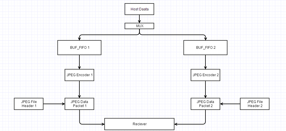
Another idea is a simple brute force technique, use two core instead of one. But the problem is this

Specific Feature Utilization:
 Number of Block RAM/FIFO:               77  out of    116    66%  
    Number using Block RAM only:         77
 Number of BUFG/BUFGCTRLs:               13  out of     16    81%  
 Number of DSP48A1s:                     21  out of     58    36%  
 Number of PLL_ADVs:                      4  out of      4   100%  

Already 66% of RAM /FIFO resource has been used. The synthesis report of only the JPEG core looks something likes this regarding RAM utilisation:

Specific Feature Utilization:
 Number of Block RAM/FIFO:               65  out of    116    56%  
    Number using Block RAM only:         65
 Number of BUFG/BUFGCTRLs:                2  out of     16    12%  
 Number of DSP48A1s:                     10  out of     58    17%  
The reason for high utilisation is the highly pipelined nature of JPEG core. Each block has has FIFO for storing intermediate values in a block in addition to ping pong memories for pipelining of each step of encoding. Also a line buffer is used which stores 16 lines of image and is biggest hogger of BRAMs.


Can the algorithms used in the blocks be improved?
I have completely read the codes of DCT, Zig-Zager and Quantiser. It seems the answer is no. Why?
Well DCT core does not use multiplier but ROM based look up table which makes it super efficient. When the pipe line is full, 8x8 blocks are processed in 64 cycles! Quantiser and Zigzager also take 64 cycles when the pipeline is full. This is pretty good. It is very difficult to beat this. Well done Mr Krepa!

I haven't completed reading the RLE and Huffman encoding block hence I can't comment on it right now.

Okay now I am getting bored so will add some more stuff tomorrow. Honestly I am in a sticky situation even before the coding period has started. I guess I should spend more time praying than coding now! :D